
Recently, EVGA has faced with some overheating issues with its GeForce GTX 1080 and GTX 1070. Since the first November 2016, all new GTX 1080 and 1070 are shipped with a new VGA BIOS and an improved VRM cooling. Today, we’re going to stress test the updated GTX 1070 FTW to check those improvements.
Article index:
1 – GTX 1070 FTW Gallery
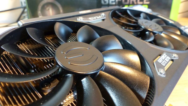
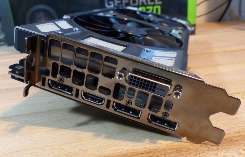
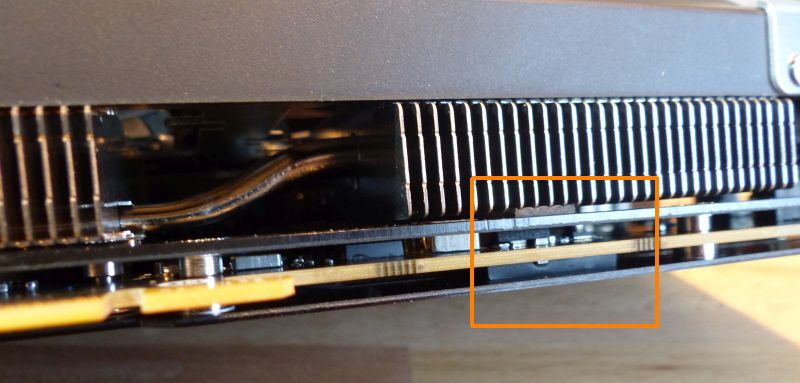
Before torturing the GTX 1070 FTW, here is a gallery of the graphics card. The EVGA GTX 1070 FTW is equipped with the third version of the ACX VGA cooler. The GTX 1070 FTW with ACX3.0 is a really nice piece of hardware. The card is heavy because of the ACX3.0 cooling system that includes a big heatsink + a memory/MOSFET cooling plate + a backplate. The PCB is literally protected by to black metallic shields. This graphics card gives you a serious feeling of robustness. The VGA cooler features two 100mm fans and like many other GTX 1070/1080, this GTX 1070 comes with the 0dB fan technology. You can also customize the RGB lighting via EVGA Precision X OC.
EVGA GTX 1070 FTW homepage: EVGA GeForce GTX 1070 FTW GAMING ACX 3.0
The bundle includes the GTX 1070 FTW, two additional power cables, a user’s guide and a gaming poster (the same poster than in the GTX 1060 SC)
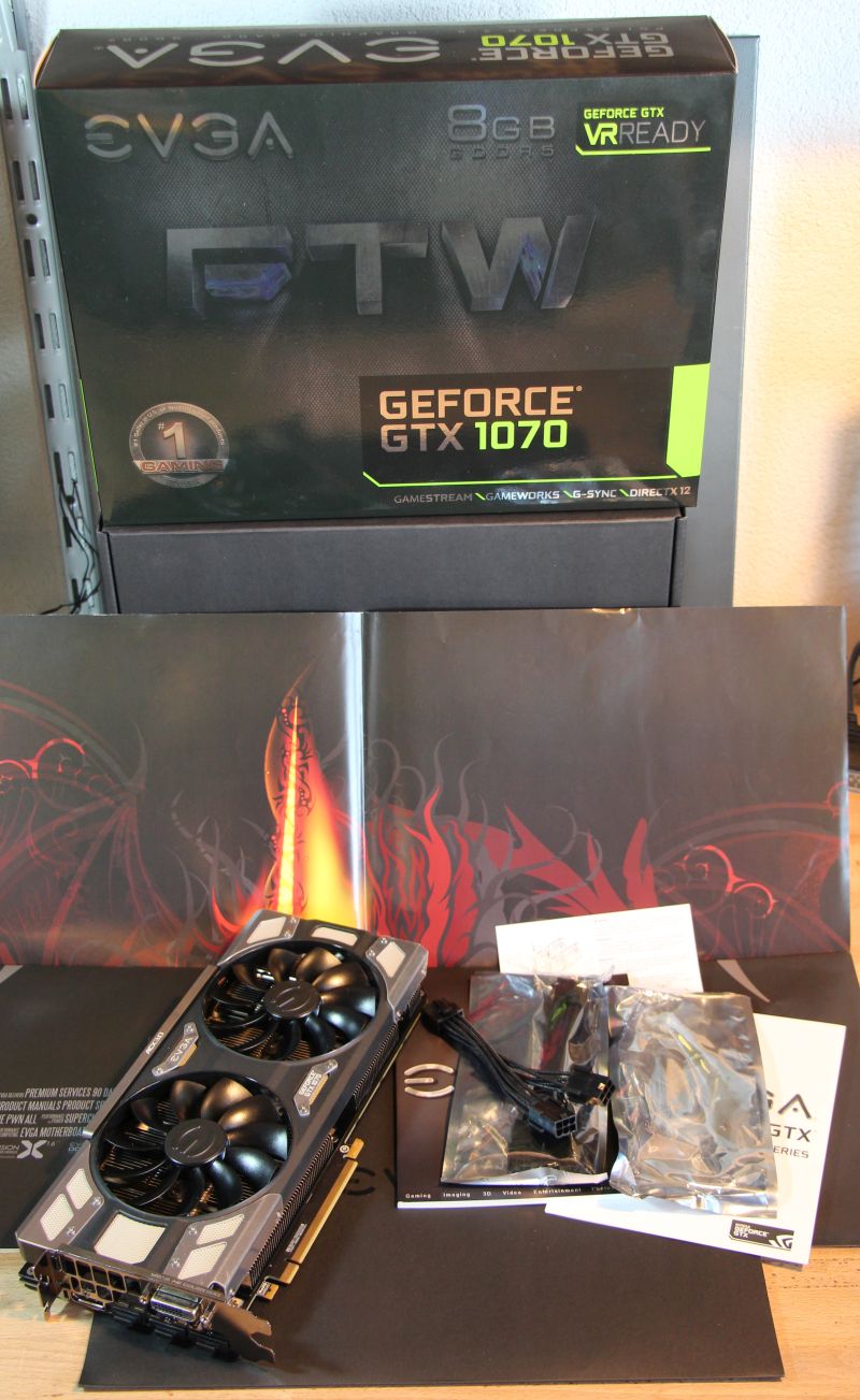


While a sticker is enough for some graphics cards makers, this is not acceptable for EVGA: the logo is etched on the fans.

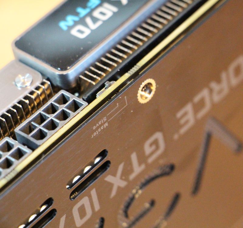
The GTX 1070 FTW requires two additional power connectors, allowing thus a max power draw of 375W for the board. The reference GTX 1070 has a TDP of 150W. The VGA cooler shroud is made up of plastic and aluminium parts.


The GTX 1070 FTW is a dual-BIOS card:
A secondary BIOS allows you to experiment with custom BIOSes without risk of breaking the card, and allows easy BIOS recovery with just the flip of a switch. Also, on select cards the secondary BIOS may unlock additional overclocking potential and/or improved fanspeed control!

The updated version of the GTX 1070 FTW comes with thermal pads on the VRMs. These thermal pads provide a better heat dissipation via the memory/MOSFET cooling plate and a backplate.
2 – GTX 1070 FTW Burn-in Test
Before any burn-in test session, I try to set the power target to the max value. The EVGA GTX 1070 FTW is a dual-BIOS card. The first BIOS (master BIOS) allows the power target to vary from +50%TDP to +112%TDP. The second BIOS (slave BIOS) unlocks more power draw with a max power target of +122%TDP.
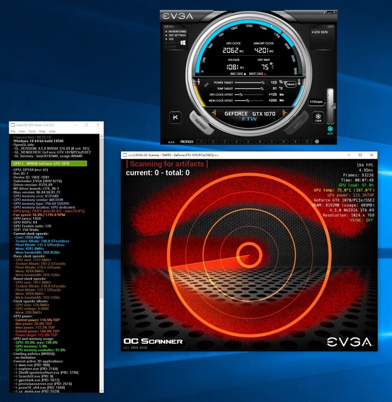
Here is a screenshot of GPU Shark with the power target information for the second BIOS:

Testbed configuration:
– CPU: Intel Core i5 6600K @ 3.5GHz
– Motherboard: ASUS Z170 Pro Gaming
– Memory: 8GB DDR4 Corsair Vengeance LPX @ 2666MHz
– PSU: Corsair AX860i
– Software: Windows 10 64-bit + NVIDIA R376.09
At idle, the total power consumption of the testbed is 43W while the GPU temperature is 32°C. The room temperature is 21°C.
To overclock the GPU core + GPU memory and stress test the GTX 1070 FTW, I used EVGA’s Precision X OC + OC Scanner.
I enabled the artifact scanner, set a resolution of 1024×768 and ran the FurMark stress test with the EVGA logo 😉
With the master BIOS and a power target limited to +112%TDP, the GPU temperature reached a max value of 72°C for a total power consumption of 300W.
With the slave BIOS, we have more overclocking headroom (+122%TDP) and I spent most of the time with this VBIOS. The max OC setting that gave me a stable overclocking was: GPU core offset: +120MHz and GPU memory offset: +200MHz with a VDDC of 1081mV. With these overclocking values, the GPU reached a max temperature of 75°C and the total power consumption jumped to 330W. On the following screenshot, you can see the current power target value (GPU power) in the OC Scanner window: 121%TDP…
An approximation of the graphics card power consumption is:
P = (330 – 43 – 20) * 0.9
P = 240W
where 20W is the additional CPU power draw when running the stress test and 0.9 is the PSU efficiency factor. EVGA gives a TDP of 215W for the GTX 1070 FTW.
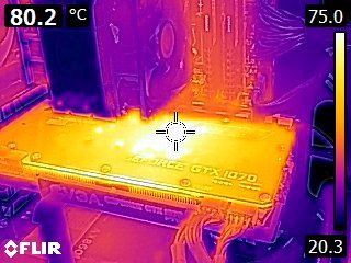
Thermal Imaging
Idle state:

Stress test – OC
3 – Conclusion
This sample of the new GTX 1070 FTW with updated VBIOS (versions 86.04.50.00.72 and 86.04.50.01.72) and thermal pads on the VRMs has no overheating issues. FurMark and all its siblings are known to put a max stress on the VRMs. This GTX 1070 FTW handled all torture tests without problem while keeping a correct GPU temperature. With overclocking settings, the max GPU temperature reached 75°C while the temperature on the backplate was around 80°C in the VRMs zone.
I didn’t use the regular FurMark like in many reviews and articles. After few tests, I saw that the new OC Scanner (available with Precision 6+) stress test was more demanding than FurMark…
I also tested the card with 3DMark benchmarks and stress tests: no problem.
What’s more, the graphics card was very quiet on load and fully noiseless at idle state. This EVGA GTX 1070 FTW is a very nice and solid product and if you had some doubts related to recent overheating issues, you can now forget them, all issues have been fixed. EVGA is back!
